Efficient PCB Heat Dissipation: A Key to Reliable Electronics

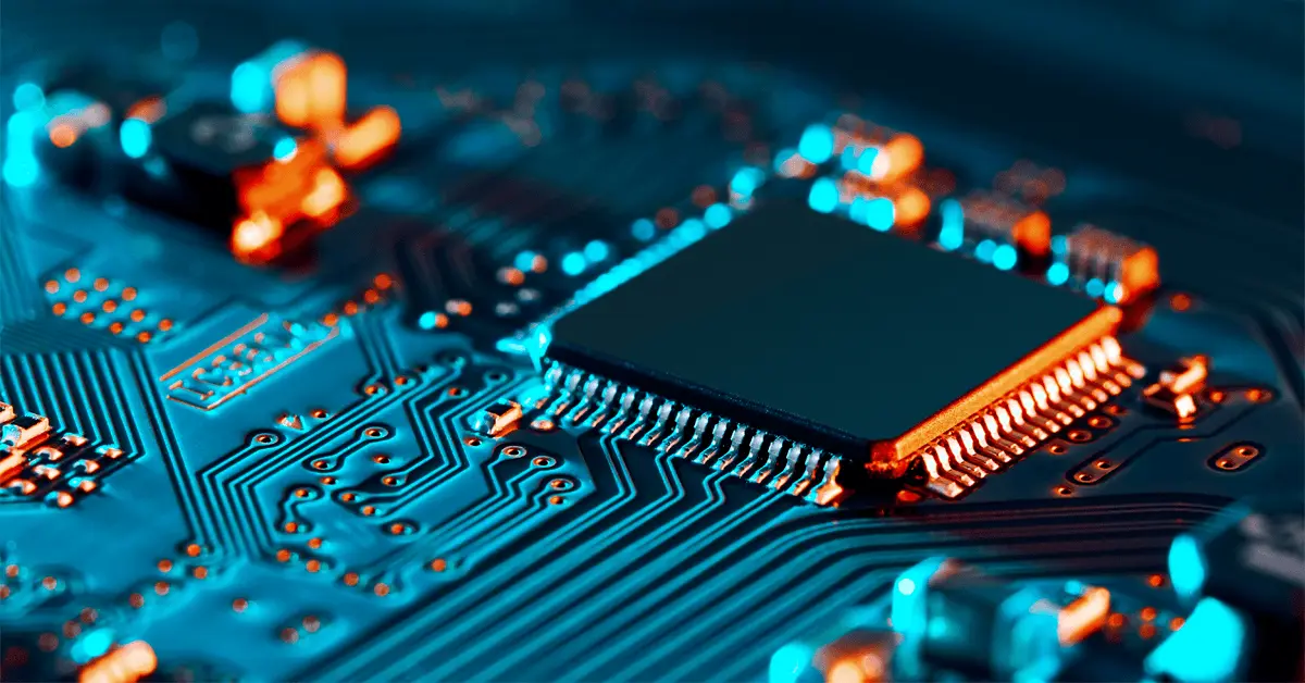
As electronic devices become more compact and powerful, managing the heat generated by densely packed components is more critical than ever. One of the major concerns in circuit design today is PCB heat dissipation, which refers to the process of removing excess thermal energy from printed circuit boards to ensure long-term reliability and performance. Without effective thermal management, components can overheat, leading to failure, degraded performance, or reduced lifespan.
There are several methods engineers use to enhance PCB heat dissipation. These include incorporating thermal vias, using thicker copper layers, employing heat sinks, and selecting thermally conductive substrates. The placement of components and overall layout design also significantly influence how well heat is distributed and expelled from the board. High-power components are typically placed in areas with the best airflow or closest proximity to heat sinks or thermal pads.
Another important aspect of thermal and electrical performance in PCBs is wire bonding, especially in advanced packaging and high-frequency applications. Wire bonding is used to connect the silicon die to the package or directly to the PCB using fine wires made of gold, aluminum, or copper. Although it’s often associated with semiconductor packaging, wire bonding also plays a role in PCBs where precision and minimal signal loss are required.
Combining effective PCB heat dissipation strategies with robust interconnection techniques like wire bonding helps ensure that modern electronic systems can operate safely under high-performance conditions. As electronic devices continue to evolve, thermal management will remain a top priority for designers looking to maximize efficiency and durability.
Frequently Asked Questions
Q1. What are the most effective PCB design techniques to improve heat dissipation in high-power applications?
A: Key techniques include using thermal vias to transfer heat to inner or opposite layers, incorporating thicker copper layers (e.g., 2 oz or more), optimizing component placement for airflow, and using heat spreaders or metal-core PCBs. These methods help lower thermal resistance and maintain consistent operating temperatures.
Q2. How does the choice of substrate material influence PCB heat dissipation?
A: Substrate materials with higher thermal conductivity, such as aluminum-backed or ceramic-filled laminates, significantly improve heat dissipation compared to standard FR-4. Material selection is critical in applications like power electronics or LED lighting where thermal loads are high.
Q3. What is the role of thermal vias, and how should they be implemented in a PCB?
A: Thermal vias are vertical conductive paths (typically filled or unfilled copper-plated holes) that channel heat from the top layer to internal copper planes or to the other side of the PCB. For optimal performance, they should be placed directly under heat-generating components and filled or capped to maintain surface planarity if needed.
Q4. How does wire bonding relate to PCB heat dissipation in advanced assemblies?
A: While primarily used for electrical interconnection, wire bonding can influence thermal paths in multi-chip modules or chip-on-board (COB) assemblies. Minimizing bond wire length and using thermally conductive encapsulants in bonded areas can enhance overall heat transfer efficiency.
Q5. What simulation tools or methods are commonly used to model heat dissipation in PCBs?
A: Engineers use thermal analysis tools like ANSYS Icepak, COMSOL Multiphysics, or SolidWorks Flow Simulation to model heat flow, temperature distribution, and airflow. These tools allow prediction and optimization of heat dissipation strategies during the design phase.


