The Role of Visual Inspection in Ensuring PCB Quality

Printed circuit boards (PCBs) are the invisible yet essential foundation of contemporary electronics. Every electronic device used today, from wearables to complex aerospace controls, depends on high-quality PCBs for precise, reliable operation. Even the slightest imperfection, such as a barely visible solder bridge or an undetected micro-crack, can trigger larger problems. Product malfunctions often lead to expensive repairs, frustrated customers, safety hazards, and, in some cases, full-scale product recalls that can permanently damage a company’s reputation. That’s why ensuring PCB quality is considered a mission-critical priority in manufacturing. Companies continually balance advanced automation and hands-on skilled labor to create inspection processes that are as thorough as possible, preventing defects from undermining finished electronics.
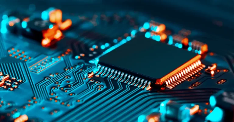
The Importance of Visual Inspection in PCB Manufacturing
Visual inspection is one of the oldest and most reliable quality control methods in electronics manufacturing. It is valued for its ability to detect surface and structural issues that automation alone might overlook. Experienced inspectors, often aided by magnification tools and specialized lighting, scan the surface and edges of PCBs, looking for specific signs of trouble: poor solder joints, component misalignment, accidental bridging, and contamination. The latest advancements in visual inspection technology, like the CAN-C reflow inspection camera Key Largo FL, have upped the ante for quality assurance. High-resolution, real-time images now allow for a comprehensive review of each solder joint and component placement, delivering faster and more accurate identification of problems before they cascade further along the manufacturing line. By capturing and analyzing these fine details, manufacturers reduce costly rework rates and better protect the functioning of their electronic products.
Key Methods: Manual Versus Automated Visual Inspection
Visual inspection in PCB manufacturing uses manual and automated methods. Manual inspection involves skilled human eyes using magnification, mirrors, and special lighting to identify hidden defects. It’s time-consuming but effective for judgment and interpreting ambiguous defects. However, fatigue can lead to missed errors. Automated optical inspection (AOI) uses advanced cameras and image processing algorithms to quickly scan PCBs for deviations from a reference image or schematic. It can rapidly, consistently, and objectively handle large production volumes, catching high-frequency issues at even the smallest scales.
Common PCB Flaws Spotted During Visual Inspection
- Solder Bridges: Unintended connections—often just a tiny sliver of excess solder—can silently link two pins, creating short circuits that may only fail after deployment.
- Misaligned or Missing Components: Placement errors from automated pick-and-place machines or manual assembly can render entire circuit sections inoperative. Even a single misplaced chip can short-circuit complex circuitry.
- Foreign Materials or Debris: Dust particles, fibers, or small metallic objects introduced during assembly or storage can, over time, create electrical shorts or corrosion sites.
- Cracked or Broken Traces: Traces are the vital highways of electronic signals. Cracks, whether from thermal cycling or physical stress, disrupt the intended flow and reliability of circuits, sometimes in ways invisible to basic electrical tests.
- Delamination or Discoloration: Signs of heat damage, moisture absorption, or adhesive failure can lead to catastrophic breakdowns, often traced back to unseen flaws at the visual inspection stage.
Early identification of these defects allows manufacturers to address root causes and implement targeted fixes, ultimately preventing widespread field failures and saving substantial time and expense in after-sales service.
How Human Expertise Adds Value
Automation and technology can speed up inspection processes, but experienced human inspectors are crucial for evaluating ambiguous issues. They can identify potential corrosion, cracks, and latent risks, and apply nuanced judgment to distinguish between benign cosmetic issues and functional red flags. The effectiveness of human inspection depends on excellent training, up-to-date knowledge of failure modes, and regular skills development. Encouraging critical thinking and communication helps manufacturers adapt to changes in component design, contaminants, or processes.
Integrating Visual Checks with Other Quality Assurance Processes
No matter how thorough, visual inspections alone are only one line of defense. To ensure the most robust PCB quality, companies integrate visual inspection with a suite of complementary testing methods:
- In-Circuit Testing (ICT): This process probes predetermined test points on a populated board for open circuits, shorts, and correct component placement, offering an electrical validation that supplements what visual checks may observe.
- X-Ray Inspection: Useful for revealing hidden solder joint flaws and voids underneath surface-mount or through-hole components—defects invisible to both manual and AOI visual inspection.
- Functional Testing: The board is powered and actively tasked with its intended functions, exposing firmware or electrical issues lurking beneath seemingly perfect surfaces.
Together, these layered testing strategies create a fail-safe environment where most faults are discovered before the product leaves the factory. Furthermore, data collected at each step allows for root cause analysis, continuous process refinement, and overall greater accountability across the production chain.
Also Read Quartist – The Fusion of Art and Technology Explained